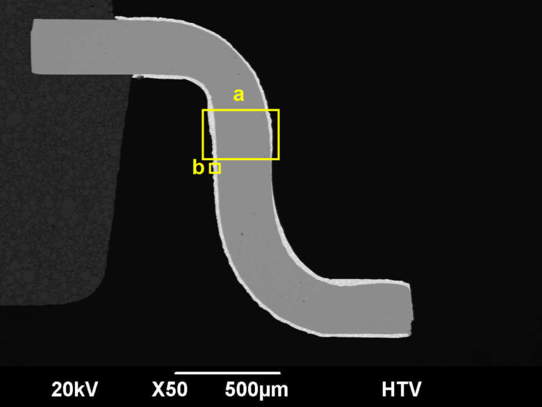
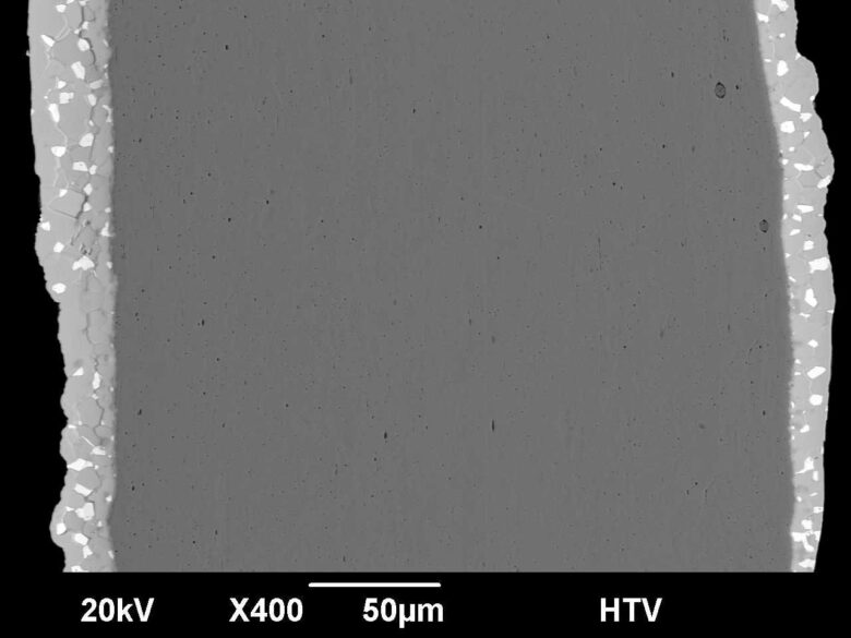
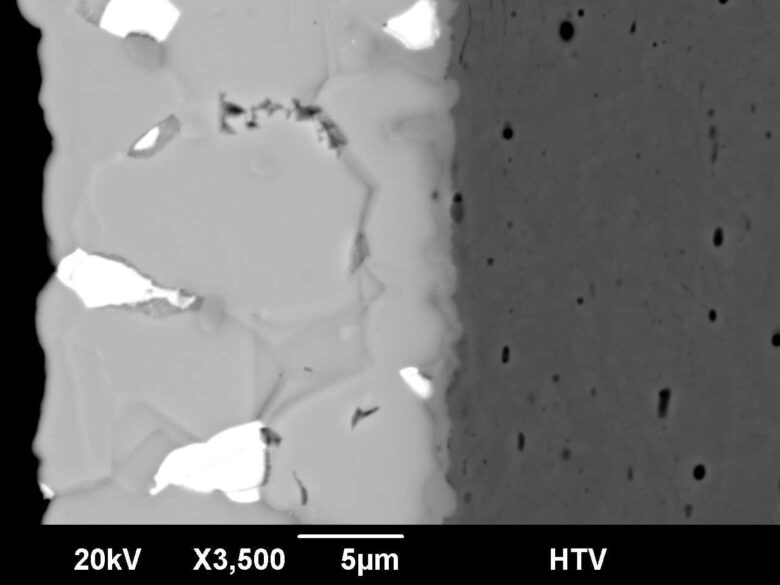
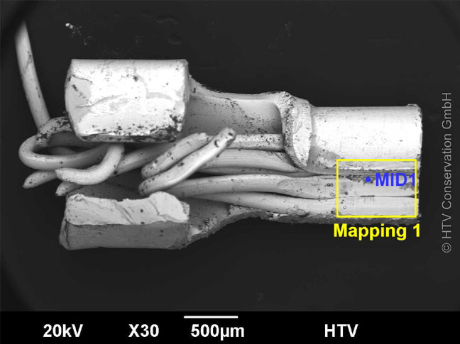
Scanning electron microscopy (SEM) to analyze structures and gradients in the nanometer range
Applied Standards
- DIN EN ISO 9220
- AS6081
Areas of application:
- Analyzing the surfaces of electronic components
- Ascertaining the layer composition of component pins and printed circuit boards
- Analyzing samples and surfaces with poor conductive features in a low-vacuum energization state
- Detection of micro fractures
- Detection of whiskers
Scanning electron microscopy is becoming increasingly important in regards to quality analyses of
electronic components, given the rising number of more and more complex component structures. The areas designated for analysis are systematically scanned with an electron beam. This causes aninteraction between the electrons and the sample, which is used to generate images of the sample magnified by a factor of 100000.
Even the most seemingly innocous samples may be analysed in regards to aging processes and
weak points or material and processing defects, using these high resolution and high quality images, allowing for thorough documentation of any flaws discovered.
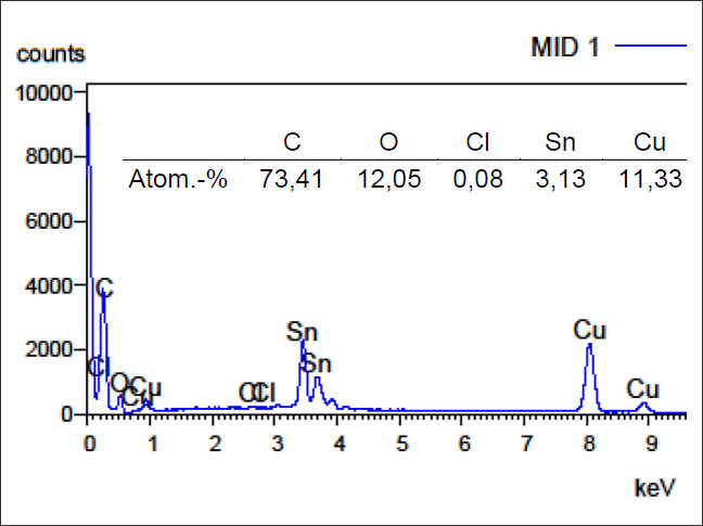
Energy dispersive x-ray analysis (EDX) to ascertain a sample’s fundamental composition
Areas of application:
- Material identification in regards to critical substances i.e., lead, as well as ascertaining their concentration
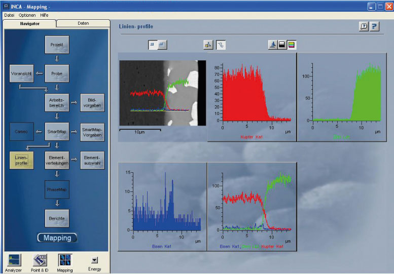
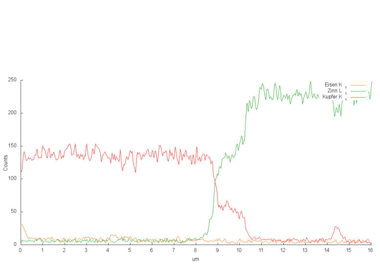
- Analyzing the diffusion progress and the transition points of different materials, i.e., measuring intermetallic phases
- Ascertaining the aging of components, i.e., their capabilities in regards to processing and storage
- Analyzing the homogeneity of materials
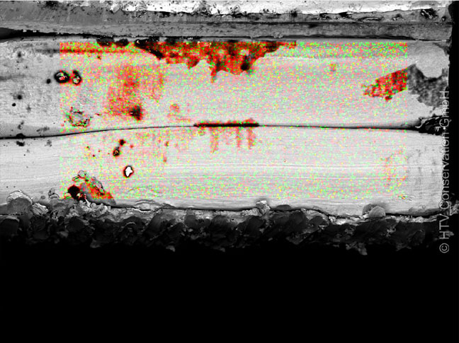
- 2D visualization of the elemental composition via mapping
Combined with SEM, the specific radiation emitted in EDX allows one to ascertain in great detail
the elements contained within the sample, their individual location as well as the components’ age
and their capabilities regarding processing and storage.


