Microsectioning and ion beam etching to visualize even the finest details on a sample’s surface
Applied standards
- DIN EN ISO 1463
- IPC-TM-650 Method 2.1.1
Areas of application:
- Visualizing of surface structures, even at the nanometer scale
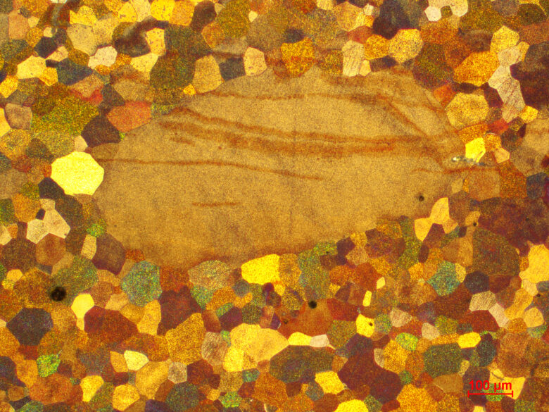
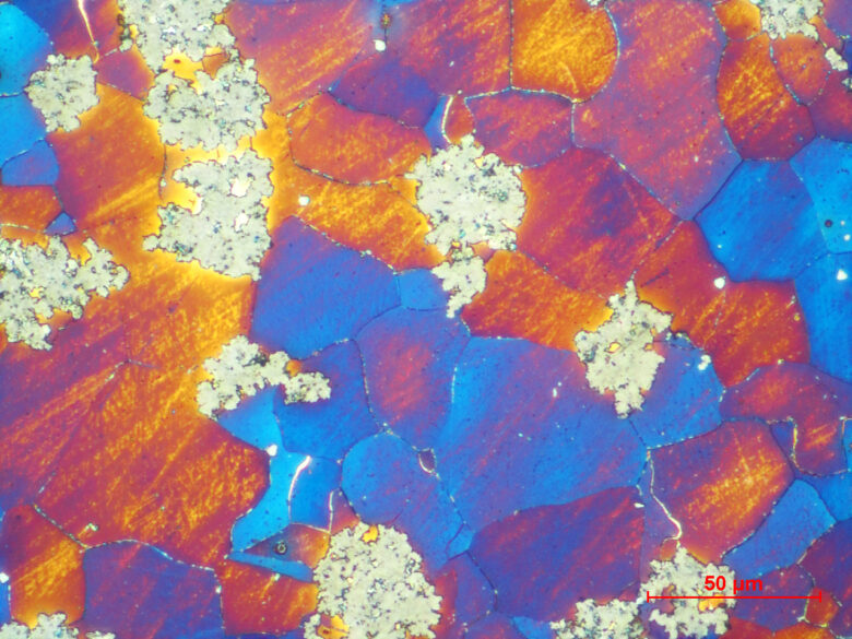
- Metallographic analysis of the microstructure
- Layer thickness determination (i.e. of component pins or the inner layers of circuit boards)
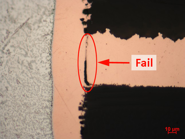
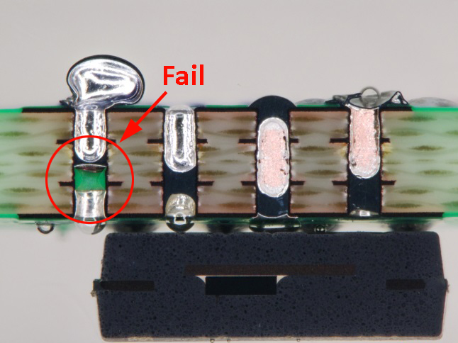
- Analysis and evaluation of solder joints, plated through holes and bonding areas
- Ascertaining thefailure mechanisms of electronic components
- Ascertaining fractures and other damages
- Printed circuit board delamination dectection
- Analysis of aging processes
- Evaluation of press-fit pins’ contact surfaces in plated through holes
- Solder joint analyses
- MetaFinePrep® for the sample preparation of very difficult materal combinations Z
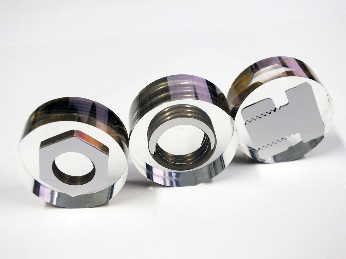
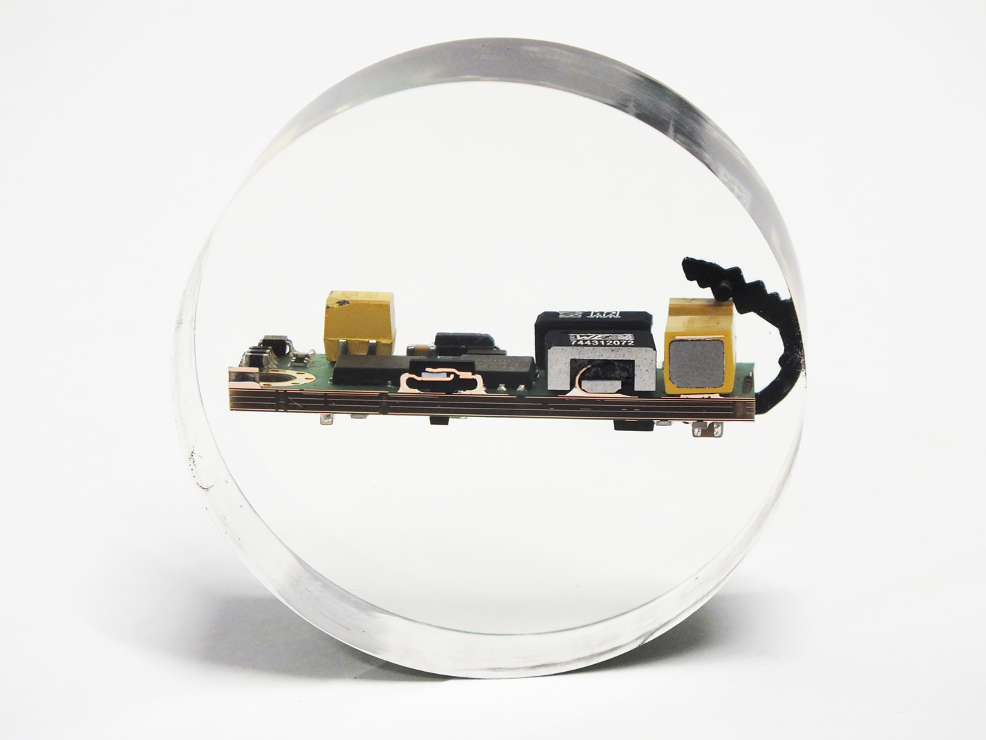
Microsectioning is a sensible addition to the light microscopy analysis to analyse the interior of electronic components, assemblies, printed circuit boards as well as any kind of metallic material.
The sample is separated with a highly precise cut along a predetermined cutting line, then, following an embedding in specialized resin, prepared for further analysis with grinding and polishing in accordance with sample specific recipies.
Microsectioning allows one to verify fracture formations along pre-existing flow and weld seams, as well as a fractographic analysis in the failure area of a housing. Additionally, glass fiber reorientations may be analyzed in the fiberglass of plastic material.
Metallograpy examples
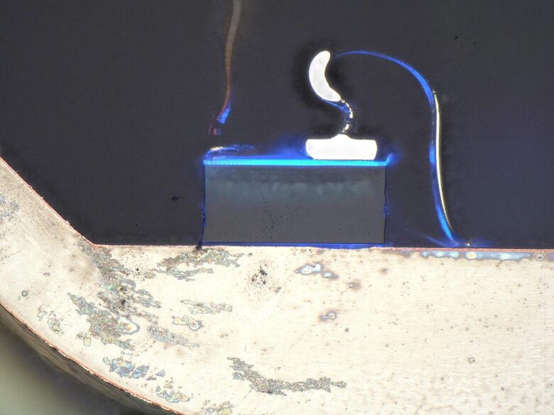
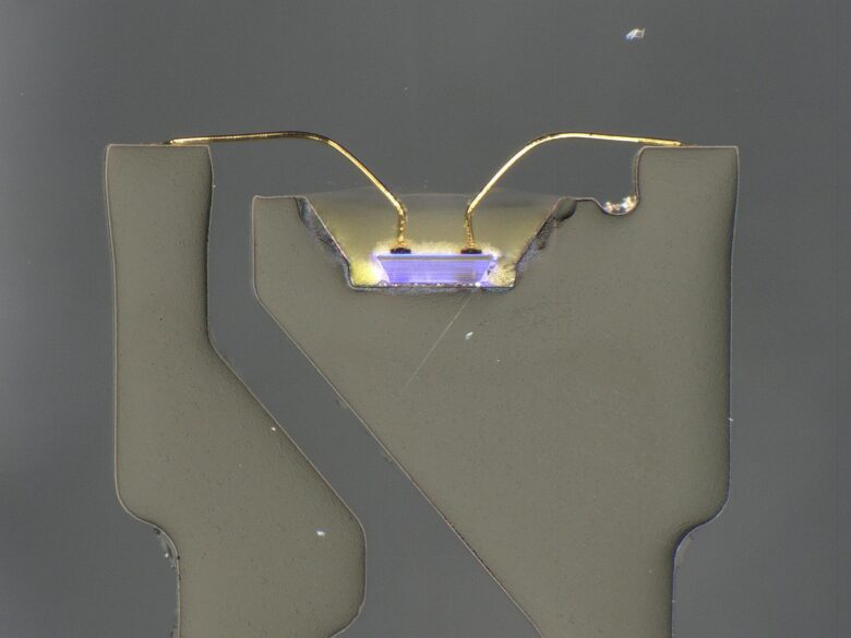
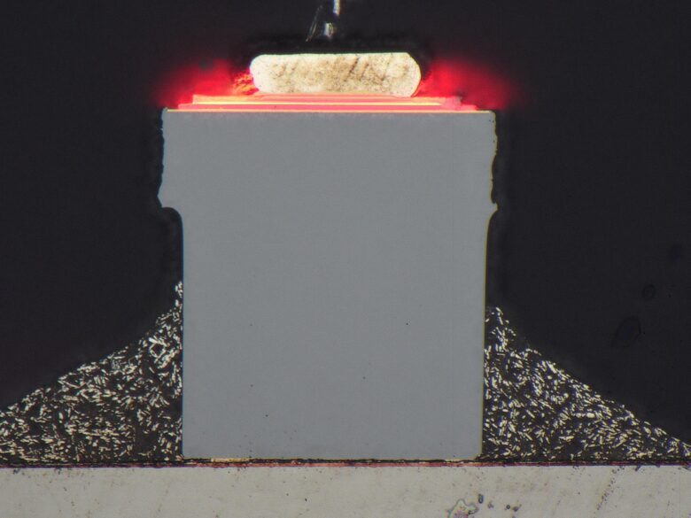
LED microsectioning examples
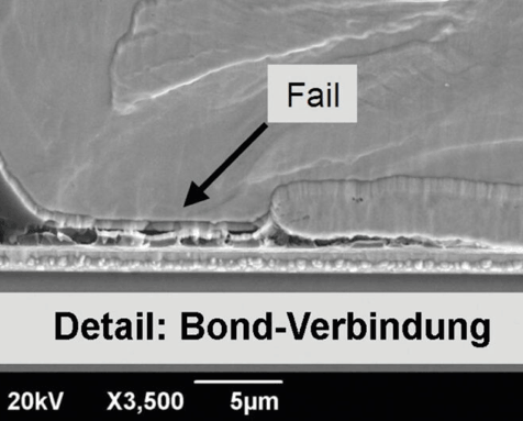
Additionally, using ion beam etching, material of a microsection sample may be removed at the atomic level. This removes possible smudges and makes even the smallest details visible. Following this, samples prepared in the described manner can by further analyesed in the nanometer range, using a scanning electron microscope (SEM), for example.
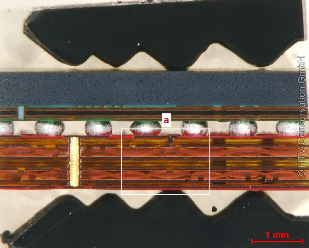
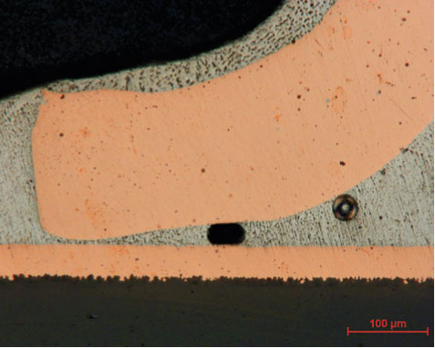
Examination of the microvia in an electronic component based on the micrograph.
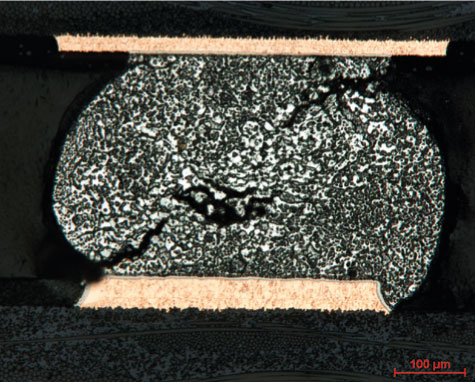
Detection of connection defects in BGA solder connections and SMD connections.
Electronic component defect examples
